The new device keeps the high-frequency switching benefits of GaN while addressing the historical lack of a true reverse body diode.
Infineon recently announced a new lineup of GaN transistor offerings that include an integrated Schottky diode. The company designed the new products, based on its CoolGaN technology, to solve GaN’s historical lack of a reverse body diode. This feature has previously limited the performance and efficiency of GaN in certain operating regions. The new CoolGaN Transistor G5 with an integrated Schottky diode reportedly "introduces a new world of possibilities for industrial applications."

CoolGaN Transistor G5. Image used courtesy of Infineon
CoolGaN Transistors G5 With a Schottky Diode
Infineon's normally-off, enhancement-mode GaN transistor combines a 100-V, 1.5-mΩ device with a co-packaged Schottky diode in a 3 mm x 5 mm PQFN package. By integrating the diode directly into the transistor, Infineon aims to reduce reverse conduction voltage and eliminate the need for discrete external Schottky components. Such integration can minimize power loss during third-quadrant operation (for example, during controller deadtime) when conventional GaN devices suffer from elevated reverse conduction losses due to high threshold and gate bias dependencies.

The new device merges the benefits of CoolGaN with those of a Schottky diode. Image used courtesy of Infineon
With these features, the new transistors target applications such as intermediate bus converters in data centers, telecom power bricks, synchronous rectifiers in USB-C chargers, and motor drive inverters. In these use cases, the reduction of deadtime loss directly improves system efficiency. It also expands compatibility with a wider range of high-side gate drivers and relaxes controller requirements to simplify circuit design and shorten development cycles.
GaN and Third-Quadrant Operation
Unlike silicon MOSFETs, GaN FETs do not possess an intrinsic body diode. This absence fundamentally alters their behavior during third-quadrant operation—the mode in which the drain becomes negative relative to the source and current flows in reverse through the device.
In a silicon MOSFET, the body diode handles reverse conduction in this quadrant, exhibiting defined reverse recovery behavior and a relatively low forward voltage drop. GaN devices lack such a structure and instead rely on channel conduction under negative drain-source bias once the gate threshold is exceeded in the reverse direction.
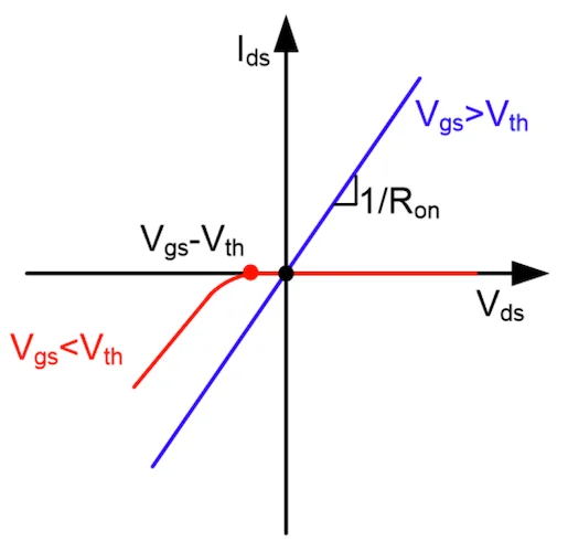
Simplified behavior of GaN in the first and third quadrants. Image used courtesy of Texas Instruments
This mechanism introduces several challenges. First, reverse conduction in GaN FETs typically results in a higher forward voltage drop (often between 2 V and 3 V) compared to approximately 0.7 V to 1 V in silicon body diodes. Second, and more critically, the absence of a body diode means GaN devices have no reverse recovery charge (Qrr). While this eliminates one common source of switching loss in silicon MOSFETs, it also means that reverse conduction losses during dead time, when both high-side and low-side switches are off, become significantly higher. These losses are exacerbated in hard-switching topologies when deadtime intervals are long or unavoidable due to controller limitations.
Ultimately, the lack of a soft, diode-like conduction path introduces sharp transitions and elevated conduction losses that degrade overall efficiency and thermals. Without a reverse-recovery diode to clamp voltage transients, designers face increased difficulty managing system-level EMI and voltage ringing.
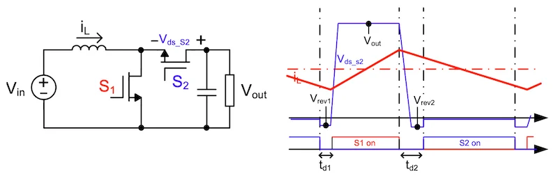
Third-quadrant behavior of a boost converter. Image used courtesy of Texas Instruments
To compensate, many designs add external Schottky diodes in parallel with GaN FETs, which increases component count, layout complexity, and cost. Thus, the lack of a reverse recovery body diode, while inherent to GaN’s structure, imposes design penalties in applications that require bidirectional current handling or experience frequent commutation.
A New Lease on GaN
GaN has always been hailed for its superior electrical and thermal performance but has also been limited by its inherent lack of a reverse body diode. With the new CoolGaN Transistor G5 with an integrated Schottky diode, Infineon hopes to eliminate the negative and amplify the positive so industrial applications can truly realize the benefits of GaN technology. Engineering samples of the new device are available now.