The release marks Renesas' first AEC-Q100-qualified Bluetooth Low Energy SoC, offering a high level of integration and power efficiency.
Renesas has released its first AEC-Q100-qualifiedBluetooth Low Energy (LE) system-on-chip (SoC) to meet the rugged demands of automotive environments.
Today’s cars rely more than ever on wireless systems for functions like tire pressure monitoring, remote entry, and onboard diagnostics. However, squeezing high-performance components into tight spaces without draining the battery or causing overheating remains a headache for engineers, especially with the strict quality benchmarks of automotive-grade electronics.
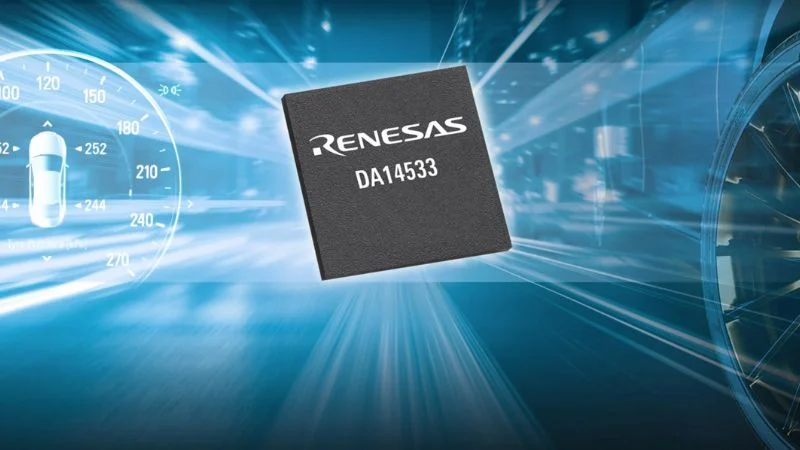
Renesas new BLE SoC, the DA14533.
More than just a Bluetooth chip, Renesas' new DA14533 (datasheet linked) combines a 2.4-GHz radio transceiver, a power-efficient Arm Cortex-M0+ processor, memory, and an array of digital and analog interfaces—all inside a tiny 3.5-mm square package.
Why AEC-Q100 Qualification Matters
For components like the DA14533 to survive in cars, they need more than just good specs—they need proven reliability. AEC-Q100, developed by the Automotive Electronics Council, has set the bar for integrated circuit (IC) durability under extreme conditions. The DA14533 currently achieves a Grade 2 certification, which means that it has been tested to operate from -40°C to +105°C.
The AEC-Q100 qualification is not just about temperature. The qualification also means the chip has passed rigorous electrical stress tests and aging simulations. This helps automakers avoid costly recalls or dangerous component failures.
Big Integration, Small Footprint
The DA14533 is highly integrated, a boon for developers trying to build efficient, reliable systems. The DA14533 incorporates a 32-bit Arm Cortex-M0+ processor running at 16 MHz, 64 KB of RAM, 12 KB of programmable memory, and a wide range of built-in peripherals—including UART, SPI, I²C, a three-channel ADC, and even a keyboard controller.
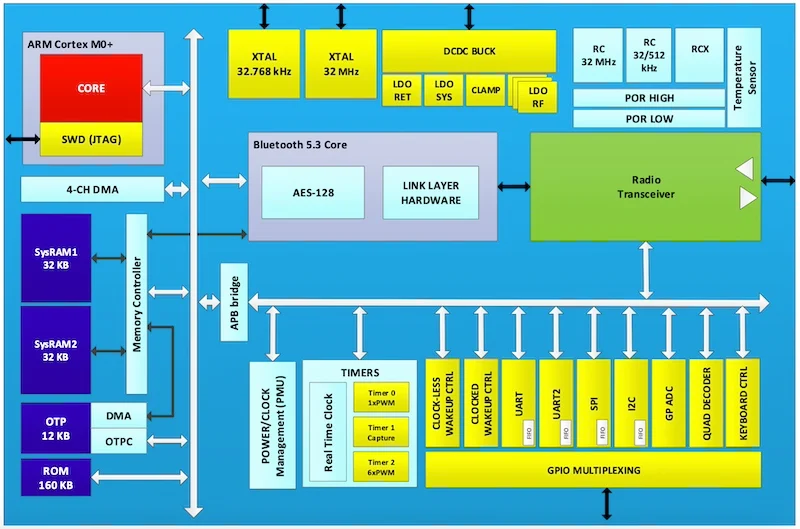
Block diagram of the DA14533.
What does this mean in practice? Fewer external components. The DA14533 only needs six supporting parts to function, which slashes the bill of materials (BOM), simplifies PCB design, and speeds up the time to market. Developers no longer have to cobble together multiple chips to get Bluetooth, processing, and memory in one system. With its ultra-low-power modes, drawing as little as 500 nA during hibernation, this chip has been specifically designed for battery-sensitive use cases like tire sensors or remote access systems.
A Smarter, Smaller Building Block
Renesas has already shipped millions of Bluetooth LE chips for industrial applications, and the DA14533 brings that same engineering approach to automotive and harsh-environment use cases. It includes features like a dedicated AES-128 encryption processor and support for up to three simultaneous Bluetooth connections, making it ready for more complex use cases.
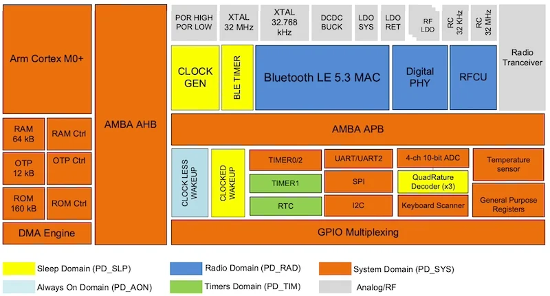
The DA14533's digital power domains.
Its onboard DC-DC buck converter actively adjusts voltage output based on load, further reducing energy waste. That kind of efficiency, paired with a compact design, makes it easier for automakers and industrial designers to build smarter, lower-cost wireless systems in tight spaces.
Designers building wireless systems for cars face constant pressure to do more with less—less space, less power, and less time. With the DA14533, Renesas delivers a tightly integrated, power-conscious SoC that meets the rugged requirements of automotive environments without adding design complexity or cost.
All images used courtesy of Renesas.